Datei:Wafer flats convention v2.svg

Originaldatei (SVG-Datei, Basisgröße: 150 × 150 Pixel, Dateigröße: 13 KB)
![]()
Diese Datei und die Informationen unter dem roten Trennstrich werden aus dem zentralen Medienarchiv Wikimedia Commons eingebunden.
![]()
Beschreibung
| Beschreibung |
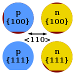
Wafer flats convention, based on Image:Wafer flats convention.PNG Conventional meaning of flats in semiconductor wafers. Red denotes material that has been removed. Wafer orientation is the orientation of the crystallographic plane in which the crystal grew. Wafer type indicated the type of doping.
|
| Datum | |
| Quelle |
self-made, Diese W3C-unbestimmte Vektorgrafik wurde mit Inkscape erstellt . |
| Urheber | Twisp |
| Andere Versionen | Wafer flats convention.PNG |
Lizenz
| Ich, der Urheberrechtsinhaber dieses Werkes, veröffentliche es als gemeinfrei. Dies gilt weltweit. In manchen Staaten könnte dies rechtlich nicht möglich sein. Sofern dies der Fall ist: Ich gewähre jedem das bedingungslose Recht, dieses Werk für jedweden Zweck zu nutzen, es sei denn, Bedingungen sind gesetzlich erforderlich. |
Dateiversionen
Klicke auf einen Zeitpunkt, um diese Version zu laden.
| Version vom | Vorschaubild | Maße | Benutzer | Kommentar | |
|---|---|---|---|---|---|
| aktuell | 23:40, 24. Sep. 2013 | | 150 × 150 (13 KB) | Cepheiden | fixed position of secondary flat Silicon processing for the VLSI era - Vol. 1 - Process technology; S Wolf; RN Tauber - Lattice Press; 1986; ISBN 096167237; p. 23 |
| 02:37, 23. Dez. 2008 |  | 150 × 150 (13 KB) | Inductiveload | Added arrow indication <110> direction and enlarged flats so they can be easily seen | |
| 23:17, 29. Feb. 2008 |  | 150 × 150 (9 KB) | Twisp | ||
| 23:13, 29. Feb. 2008 |  | 150 × 150 (9 KB) | Twisp | ||
| 23:06, 29. Feb. 2008 |  | 150 × 150 (8 KB) | Twisp | ||
| 22:59, 29. Feb. 2008 |  | 150 × 150 (8 KB) | Twisp | ||
| 20:09, 29. Feb. 2008 |  | 150 × 150 (9 KB) | Twisp | {{Information |Description= Wafer flats convention, based on Image:Wafer flats convention.PNG Conventional meaning of ''flats'' in semiconductor wafers. Black denotes material that has been removed. Wafer orientation is |
Dateiverwendung
Die folgenden 2 Seiten verwenden diese Datei:
Globale Dateiverwendung
Die nachfolgenden anderen Wikis verwenden diese Datei:
- Verwendung auf ca.wikipedia.org
- Verwendung auf cs.wikipedia.org
- Verwendung auf en.wikipedia.org
- Verwendung auf es.wikipedia.org
- Verwendung auf et.wikipedia.org
- Verwendung auf eu.wikipedia.org
- Verwendung auf fi.wikipedia.org
- Verwendung auf it.wikipedia.org
- Verwendung auf it.wikibooks.org
- Verwendung auf ja.wikipedia.org
- Verwendung auf ko.wikipedia.org
- Verwendung auf nl.wikipedia.org
- Verwendung auf pl.wikipedia.org
- Verwendung auf ro.wikipedia.org
- Verwendung auf sk.wikipedia.org
- Verwendung auf uk.wikipedia.org
- Verwendung auf www.wikidata.org